
By creating 40,000 user-defined defects in a single crystal lattice, researchers have shown that atomic manipulation can be achieved on the mesoscopic scale – between the single-atom and bulk-material ranges. The work potentially offers a way to engineer materials with desired properties by fine-tuning the positions of individual atoms within their structures.
Scientists have known for decades that microscopy techniques can be used to manipulate the positions of individual atoms. In 1990, two IBM researchers carried out an iconic demonstration, dragging 35 xenon atoms across a nickel surface to spell out the company’s name.
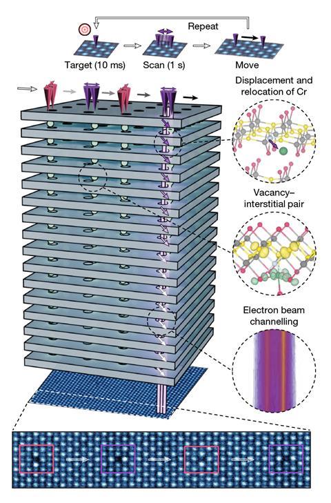
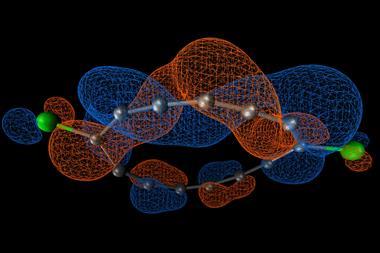
Now, a team from the US and Europe has scaled up the concept to a whole new level. Using the electron beam in a specially programmed scanning transmission electron microscope, the researchers introduced 40,000 defects into a chromium sulfur bromide lattice. The CrSBr semiconductor was selected as a model sample and, with their automated process, the researchers could subtly reposition individual chromium atoms in a predictable manner. They describe the resulting material as ‘a new form of engineered artificial matter’, and note that it remains stable at room temperature outside of the microscope.
The defects were introduced within minutes across an area measuring 150nm × 100nm with a depth of 13nm. However, the team believes that the method is generalisable and could be scaled up to the macroscopic level. The researchers write that the technique offers a new way to produce programmable matter in which ‘functionality is engineered from the atom up’.
References
J Klein, et al, Nature, 2026, DOI: 10.1038/s41586-026-10431-9


No comments yet