Can anything replace the silicon in our mobile phones and laptops? The hunt is on, reports Hayley Bennett
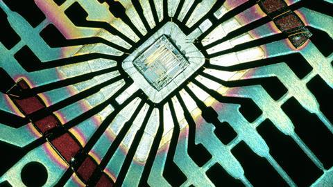
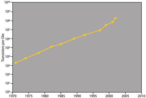
In 1965, an errant US chemist made a prediction about the future of the computing industry. Gordon Moore, who had earned his PhD in physical chemistry at the California Institute of Technology, turned his attention to electronics and founded a company that made some of the first silicon chips. His prediction: that the number of components it was possible to cram onto a computer chip would double every year as the components became teenier and tinier, yielding rocketing computing power. Although Moore later revised his prediction to every two years, it held true. Until round about now. Intel can squeeze 100 million transistors, which have shrunk to nano-proportions, onto each square millimetre of its chips, but the industry’s ability to keep up with Moore’s Law – as it’s widely known – is starting to flag.
The quest to build ever more powerful computers gets us into the realms of quantum computing and adding extra dimensions to chip architectures. But in the meantime, could using alternative materials help to prolong Moore’s Law? Right now, materials scientists are trying to help chip designers take transistors to their physical limits by replacing the very substance that the computer chip industry is built on – silicon. As Eric Pop, an electrical engineer and materials scientist at Stanford University in the US sees it, those people who are saying Moore’s Law is dead are too stuck on silicon. ‘What they’re referring to is the fact that it’s very, very difficult to shrink silicon circuits,’ he says. ’But if you switch from silicon to a material that is [a few] atoms thick, at least for certain parts of the chip, you could make those circuits 10 times smaller.’
What Pop is talking about is already happening to some degree. Modern silicon chips often contain ‘sprinklings’ of other materials, such as silicon–germanium alloys, gallium arsenide and hafnium dioxide, all used judiciously to complement the otherwise ubiquitous silicon and silicon dioxide. Meanwhile, scientists are working to produce smaller transistors from atomically thin crystals of molybdenum disulfide and black phosphorus. In combination with multi-layered designs for chips, new materials could lead to a thousand-fold gain in computing speed and energy efficiency.1 The question is whether such exotic materials will be accepted by the semiconductor industry, whose response, according to Pop, is always ‘That’s great, but how the heck are we going to incorporate this into silicon?’ Faced with the demise of Moore’s Law, perhaps it’s about time they found a way.
Stuck on silicon
At the nanoscale, silicon circuits start to become inefficient, leaking current and heat. So why is the industry still so stuc using silicon when they can’t go any smaller with it? Well, aside from the fact that it’s the second most abundant element on Earth, it’s simply the way things have always been done. Making the switch would be a hassle – and an expensive one. ‘The reason silicon is so difficult to replace is that all the processes in companies like Intel are geared towards silicon,’ says Justin Holmes, a nanochemist leading a materials group at University College Cork in Ireland. ‘You can imagine the billions of dollars it costs in terms of equipment, so the last thing they want to do is move away from silicon.’
So there’s a cost issue, but why is silicon itself any good? What do new materials have to match up to? One of the key parameters for a transistor material is its band-gap – a measure of the material’s conductivity, based on the amount of energy it takes for electrons in the material’s atoms to enter a conducting state. In transistor terms, thinking of a transistor as a simple switch, the band-gap determines the amount of energy required to switch it on. Too high (as in most insulators) and you waste a lot of energy turning the transistor on; too low and the electrons jump too easily into the conduction state, resulting in a leaky transistor that loses current. So one good thing about silicon is its mediocrity. At 1.1 eV, its band-gap isn’t too high or too low. That’s what makes it a semiconductor, in fact.
The last thing they want to do is move away from silicon
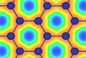
The reason that the one-atom-thick, all-carbon material graphene – once touted as the saviour of Moore’s Law – hasn’t really made it big in computing yet is that isn’t actually a semiconductor. It has a zero band-gap, meaning its electrons flow at any energy level. So it might make really speedy transistors, but you can’t switch them off. Although as Holmes explains, there are ways of getting around this: ‘You’ve got to have a band-gap, which means that you have to process the material. [For instance], there are devices that are using graphene ribbons.’ Ribbons of graphene thinner than 10 nm wide, it turns out, do behave more like semiconductors. However, inspired by graphene, researchers are now looking at other ultra-thin semiconductors as potential alternatives to silicon.
Turning to 2D
The advantage of these 2D materials is not just that they reduce the thickness of chip components, but that they allow us to make the transistor smaller in another direction too. In a transistor, the channel – the part of the transistor where the current flows between source and drain – is what determines length. A gate over that channel controls whether the current flows or not. This forms the switch. As silicon circuits have shrunk in line with Moore’s Law, the source and drain have moved closer and closer together until they are just nanometres apart, eventually leading to current leaking between them even when the ‘switch’ is supposed to be off. In 2D materials, this situation is remedied by the flow of electrons being confined within an ultrathin channel, meaning each electron is influenced in the same way by the electric field of the gate.2
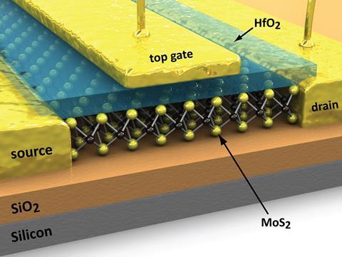
Pop’s team has recently been injecting a lot of work into single-layer-thick molybdenum disulfide (MoS2), one of a class of materials known as transition metal dichalcogenides (TMDs). TMDs are particularly good at having the current flow when it’s supposed to and stopping it when it’s not, as evidenced by their ‘on–off’ ratio, which is orders of magnitude higher than silicon. Structure-wise, Pop describes them as ‘a sandwich where the bread is sulfur, selenium or tellurium and the filling is a heavy metal’. So his ‘moly disulfide’, as he affectionately refers to it, is a three atom-thick layer comprised of a molybdenum filling between two sulfur crusts. It has a ~1.8 eV band gap and although it’s not atomically thin in the way that graphene is, it’s pretty close.3 The first few/single-layered MoS2 was fabricated in the 1960s using sticky tape to peel single layers of the material off molybdenite, just as graphene was later peeled from bulk graphite. Single-layered MoS2 was eventually fabricated in transistor form in 2011 by a Swiss group,4 but working with this type of material isn’t easy. ‘What kills you is the defects in the materials,’ says Holmes. MoS2 transistors made this way can be extremely fragile and difficult to handle.
Now, though, Pop’s group has shown it’s possible to grow large, several cm2 sheets of high-quality MoS2 crystal on a silicon substrate, using the much more precise method of chemical vapour deposition.5 Pop says the result is beautiful and relatively defect-free, but he’s acutely aware of industry’s feelings about the advance. ‘They say “Gee, these results are really nice, but even though you grew these on a separate chip, we don’t know how to transfer the material from that separate chip onto the silicon processor to make a circuit on top of it.”’ It’s a fair point. Handling 1cm2 of this stuff, which is less than a nanometre thick, would be akin to keeping hold of a piece of cling film the size of an athletics track. But it also reveals how industry currently views alternatives to silicon – as complementary rather than a complete replacement. Pop hopes industry will step in to fund research on better ways to transfer the ultrathin materials or grow them at lower temperatures so they can be formed directly on top of the silicon circuitry without destroying it.
Hot for hafnium
It’s not just the silicon channel that could benefit from an upgrade. Take the silicon dioxide insulator used as a gate material. It’s not really that great once you get down to nanometre scales, because if it’s too thin, it’s easy for electrons flowing through the channel to ‘tunnel’ through it. But it does need to be very thin to scale with the extremely short, thin channels of state-of-the-art transistors. At the University of Kentucky in the US, Beth Guiton’s team is attempting to replace the gate material with a very particular crystal form of hafnium dioxide, and Guiton is ‘really excited’ about it. What she’s excited about has to do with the material’s combination of high band-gap even when it’s super-thin, which helps prevent tunnelling, and high ‘ĸ value’, which allows precise control of the gate and device switching, as Guiton explains, thus improving performance. It’s unusual to find a material that has both. The ĸ value of silicon dioxide is only 3.9. Normal, regular hafnium dioxide has a ĸ value around 18 – hence why it’s already been adopted by the semiconductor industry and is probably already in your mobile phone – but the exotic form of hafnium dioxide that has Guiton so keyed up has a calculated ĸ value of 75 and that’s what makes it very attractive for transistors.
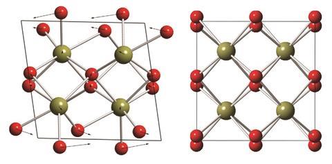
According to Guiton, the only structural difference between the exotic stuff (tetragonal) and the regular stuff (monoclinic) is a tiny displacement of the hafnium and oxygen atoms – no bonds are broken or formed so it takes very little energy to get from one phase to the other. There’s just one problem: it’s only stable at a temperature higher than molten lava (1700°C). Usually, such high temperature phases can be ‘frozen in’ at room temperature and they don’t transform back because the energy required is too great. But for tetragonal hafnium dioxide the energy required for the tiny displacement of atoms is so small that hardly any energy is required at all. ‘So if we opened up a furnace that contained tetragonal hafnium dioxide and took that out and plunged it into liquid nitrogen, it would still transform to the monoclinic phase,’ explains Guiton. ‘You can’t trap it, you can’t freeze it.’ It doesn’t sound like something that is going to work well in a computer chip at room temperature. Guiton’s collaborators at Texas A&M University have, however, successfully synthesized hafnium dioxide in nanorod form and, as their joint paper from May this year shows, this material behaves very differently at the nanoscale.6 Under a scanning transmission electron microscope, the Kentucky group watched a single rod of hafnium dioxide transforming into the sought-after tetragonal phase at just 600°C.
The tetragonal phase starts growing at defects in the crystal called twin boundaries, like mirror planes where the crystal on either side scatters light in different directions. It also nucleates at surface atoms, which make up more of the crystal in nanorods than they do in the bulk material. The implication is not only that small enough rods will transform to the tetragonal phase at room temperature, but that controlling the number of defects in hafnium dioxide could be a way to control its crystal structure more generally. ‘If you can control the density of those defects, maybe you can use that to control the way it transforms between these phases,’ explains Guiton. It’s only an idea, but as ordinary hafnium dioxide is already being incorporated into silicon transistors as an insulator, maybe industry will be interested in pursuing the material further.
Pop hopes so too. He’s also been working with hafnium dioxide and he’s excited about it for a different reason. To return to silicon once more, one of the things that makes it so practical is that it naturally forms its own insulator, silicon dioxide, simply by coming into contact with air during the manufacturing process. Other useful semiconductors don’t do this, or they form oxides that aren’t very good insulators, meaning a separate insulating layer has to be applied. But Pop’s team fancied their chances at finding another material that behaved a bit more like silicon.
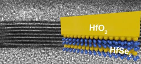
‘The fact that silicon oxidises into silicon dioxide, which happens to be a good insulator is an incredible stroke of good luck,’ Pop says. ‘So we basically went looking for 2D materials that oxidise into really, really good insulators that are already known and appreciated by industry.’ They came up with hafnium selenide (and zirconium selenide), which oxidises to form hafnium dioxide – though just the regular stuff.7 Earlier this year, they created some of the first transistors from these materials and although Pop admits they had to employ the ‘primitive’ sticky tape method to get their 2D layers, their work with moly sulfide suggests it’s just a matter of time before better processes emerge.
What all this tells us is that materials certainly do exist that are, in some respects, better than silicon. Step-by-step, we are seeing the material that has long dominated the semiconductor industry being replaced. The question is whether these new materials are being developed quickly enough to keep pace with Moore’s Law. According to Holmes, the semiconductor industry is resigned to the fact that Moore’s Law will come to a ‘grinding halt’. However, he thinks that advances in quantum computing and chip architecture, along with new materials, will yield more powerful computer chips even after the physical limits of transistor size are reached. Pop agrees that some of the really big gains in processing power will come from new chip architectures. Perhaps materials like molybdenum disulfide and hafnium dioxide can make a smaller but important contribution. When it comes to Moore’s Law, though, Pop is ever the optimist. ‘Moore’s Law’s not dead!’ he exclaims. ‘Don’t let anybody tell you that!’
Hayley Bennett is a science writer based in Bristol, UK
Black phosphorus
Until 1914, phosphorus came in two varieties: white and red. Then US physicist Percy Bridgman took the white stuff and subjected it to high pressure to make black phosphorus. Today, this mysterious-sounding material is used to make a 2D material (phosphorene) that has some intriguing properties. Firstly, the crystal structure of black phosphorus looks different in different directions. A single-atom-thick layer of phosphorene can also have different structures, which carry charge at different speeds. Secondly, and perhaps most interestingly, its band-gap is tunable depending on the number of layers – between 0.3 and 2.0 eV.7 And thirdly, as David Lewis, a materials scientist working on 2D materials at the University of Manchester, UK, explains, its electron mobility, a determining factor for computing speed, is 10 times that of the more mature 2D material molybdenum disulfide (MoS2). ‘So this really allows you to access a different suite of properties for transistors and other electronic devices,’ he says. However, with the science of phosphorene still in its infancy, it’s not without its limitations. Making phosphorene flakes currently means peeling them off black phosphorus with sticky tape, as scientists did when they first made graphene and ultra-thin MoS2. More scalable liquid exfoliation techniques are in development.8 Then there’s the small problem of it degrading to phosphates in air. According to Lewis, there have been various strategies to stabilise it, including encapsulation in materials like aluminium oxide. Besides transistors, other possible applications include water-splitting devices, solar cells and lithium-ion batteries.
References
1 M Aly et al,Computer, 2015, 48, 24 (DOI: 10.1109/mc.2015.376)
2 M Chhowalla, D Jena and H Zhang,Nat. Rev. Mater., 2016, 1, 16052 (DOI: 10.1038/natrevmats.2016.52)
3 X Li and H Zhu,J. Materiomics, 2015, 1, 33 (DOI: 10.1016/j.jmat.2015.03.003)
4 B Radisavljevic et al,Nat. Nanotechnol., 2011, 6, 147 (DOI: 10.1038/nnano.2010.279)
5 K Smithe et al,2D Mater., 2017, 4, 011009 (DOI: 10.1088/2053-1583/4/1/011009)
6 B Hudak et al,Nat. Commun., 2017, 8, 15316 (DOI: 10.1038/ncomms15316)
7 M. Mleczko et al, Sci. Adv., 2017, 3, e1700481 (DOI: 10.1126/sciadv.1700481)
7 C Chowdhury and A Datta,J. Phys. Chem. Lett., 2017, 8, 2909 (DOI: 10.1021/acs.jpclett.7b01290)
8 J Brent et al,Chem. Commun., 2014, 50, 13338 (DOI: 10.1039/c4cc05752j)


3 readers' comments