
Phosphorus is the latest element to enter flatland, where it becomes a p-type semiconductor
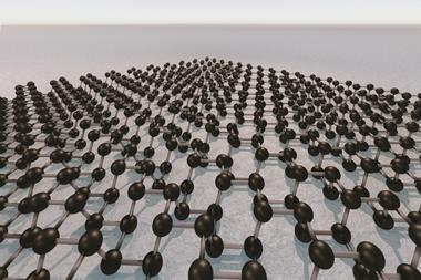
US researchers have made phosphorus into an analogue of graphene, dubbed phosphorene, allowing practical electronic devices made from such two-dimensional materials.1 Peide Ye at Purdue University, US, and his co-workers show that phosphorene is the first native 2D electron-poor – or p- type – semiconductor. That’s important for making these flat materials into standard complementary metal-oxide semiconductor (CMOS) logic circuit elements, which Ye’s team has also achieved with phosphorene. ‘For device applications it’s fundamentally better than graphene,’ Ye says.
The transistor switching in our computers and mobile devices typically relies on interfaces between p -type semiconductors and n -type semiconductors, which have an excess of electrons. As a conductor, unaltered graphene can play neither role. Flat MoS2 is an n -type material, but making two-dimensionalp -type semiconductors so far has been difficult.
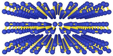
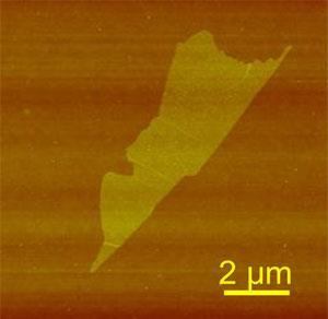
Ye got the idea to make phosphorene when a colleague told him about black phosphorus, the most stable form of the element in open air. It’s comprised of loosely bound layers, like graphite, making it possible to copy how University of Manchester’s Andre Geim and Kostya Novoselov first made graphene. That ‘Scotch tape method’ simply involves attaching tape to bulk crystals and then peeling it off. A few layers stay on the tape, but can be released with solvent. Ye and his colleagues had been using this method with MoS2, and he quickly saw black phosphorus’s potential. ‘I immediately Googled black phosphorus, and in 30 minutes I knew all that I needed to do,’ he says.
Chip leader
To fully understand the new material, Ye’s electrical engineering team hooked up with David Tománek’s theoretical physics group at Michigan State University, in East Lansing. Their calculations suggest that phosphorene has ridges that lock its layers in place. They also indicate that changing the number of phosphorene layers can alter how much energy is needed to make it conductive, a quantity known as its bandgap. That could help tailor the electronic properties of devices made with the material. Single-layer phosphorene, with the highest bandgap of all, would be especially desirable as it would ensure the clearest distinction between a transistor being on or off. ‘We’re trying all means to make that now,’ Ye says.
Having produced phosphorene, Ye’s students Han Liu and Adam Neal then made it into a p -type field-effect transistor to measure its hole mobility, or how fast charge moves in the form of positively charged absences of electrons. At 286m2/Vs this is unsurprisingly much slower than electron mobility in graphene, which is around 15,000cm2/Vs, while the ridged structure makes its performance directionally dependent. But Ye stresses this figure is ‘encouraging’ as it’s around three to five times the value for MoS2, while silicon’s hole mobility is just 100cm2/Vs. Finally, the researchers also put both MoS2 and phosphorene onto the same silicon wafer to make an inverter, the simplest CMOS circuit element.
Phosphorene’s hole mobility is its most notable property for Andrea Ferrari, director of the Cambridge Graphene Centre in the UK. But he adds that there are around 500 layered materials that could be used to extract monolayers. ‘This is an interesting addition to the growing list of 2D crystals,’ Ferrari says.
Paola De Padova from the Institute of Structure of Matter in Rome, Italy, who helped discover silicene, the 2D form of silicon, especially likes the ability to tailor phosphorene’s bandgap. However, she wants more structural and spectroscopic data, and also points out that its usefulness could be limited by the high temperatures and pressures needed to make black phosphorus. ‘It is important but, at this moment, expensive,’ she says.
Ye was not the only one to see the opportunity black phosphorus offered 2D electronics. On the same day as his team’s paper was posted on the arXiv website, Yuanbo Zhang from Fudan University and coworkers also posted similar work on the same site.2


No comments yet