


Ben Valsler
This week, Rowena Fletcher-Wood with a compound that shines a light on semiconductor science.
Rowena Fletcher-Wood
The history of gallium nitride tells of a low-efficiency, impure, problematic compound.
A relatively modern material, gallium was discovered in 1875 and instantly slotted into a gap in Mendeleev’s periodic table, exhibiting the predicted physical properties of his ‘eka-aluminium’. Gallium nitride meanwhile, rose to fame in the ‘60s, upon the growth of its first single crystal films. A combination of group III and V elements, gallium nitride is isoelectronic to the elemental semiconductor germanium, but differs in its structure and band gap. Scientists were excited to explore its properties.
One of the properties of gallium nitride was that it readily transformed electrical energy into a dim blue light, a much sort-after colour for LEDs. It was also found to be tolerant to a wide range of temperatures, resistant to ionising radiation and less reactive to the atmosphere than other group III-V compounds, making it easier to use. Crucially, it showed a low electrical resistance, losing only a small proportion of power as heat and so allowing it to handle ten times the voltage of silicon, making smaller, faster, and more efficient devices.

But though the potential of gallium nitride sounded boundless, it wasn’t. In fact, gallium nitride turned out to be extremely unreliable – and extremely inefficient, turning no more than 0.005% of electrical input into light, sixty times less than silicon carbide.
It also suffered from a major hitch: gallium nitride transistors never turned off. The neurons of computer signalling, transistors are designed to let high currents flow and block high voltages – but gallium nitride transistors flowed all the time, like a constant stream of adrenaline, risking a short circuit.
To make gallium nitride usable, both p (positive) and n (negative) doped semiconductors were needed to set up p-n junctions, the building blocks of electronics. At the junction, the charge flow from negative to positive leaves a depleted, non-conductive layer that can be manipulated to make diodes. N-type gallium nitrides are readily produced by doping with oxygen or silicon, but for many years p-types remained elusive.
The problem was one of purity. Back in the 1960s and ‘70s, production methods suffered from heavy oxygen and water contamination. Accompanying this were large numbers of dislocations to the lattice structure. The impurities added to the fabric of the band structure and so influenced semiconducting properties.
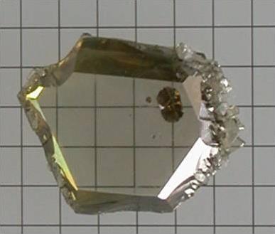
Gallium nitride has a Wurtzite crystal structure. Typically, it’s grown on sapphire crystals, which have a corundum crystal structure with the same arrangement of oxygen atoms, but a different arrangement of metal ions. Although this doesn’t cause dislocations in the product, scientists have found that growing the crystals on buffer layers of gallium arsenide, which has a zinc blende structure, actually reduces them. Modifying the structure also turned out to be the clue to off-only transistors, and suddenly gallium nitride semiconductors started to look possible.
The breakthrough came with the development of new synthetic methods. As contamination was reduced, not only was reliability improved, but n-type oxygen and water concentrations dropped off, making magnesium-doped p-type semiconductors possible. But something else changed too: they emitted light in the ultraviolet.
In fact, this makes sense for the theoretical band gap of gallium nitride, and simply wasn’t seen before in the very contaminated material. So what about the blue light? Actually, the light from magnesium-doped gallium nitride is violet, a colour we struggle to detect. The blue light is the result of electron impact excitation deep within the material.
Today, the main obstacle for gallium nitride is cost. Already, it appears in devices from blu-ray readers to photocatalysts, and is involved in the electrolysis of water. In the future, its use with LED lights could produce 70% to 80% efficiency. It could be used to make smaller laptop power adaptors , more compact solar cells on satellites, or to produce tetrahertz radiation for medical imaging, body scanning or spying. Single crystal gallium nitride nanotubes and nanowires have further applications in micro- and optoelectronics. These tiny materials, as a result of their large surface to bulk ratios, are subject to quantum effects and may have very different properties to the bulk materials.
As it becomes cheaper to make, gallium nitride could be used to run Google, detect skin cancer, and, by reducing battery weight and increasing battery capacity, it could even take you to the shops in the next generation of electric vehicles.
Ben Valsler
Rowena Fletcher-Wood with gallium nitride. Next week, Kat Arney on the popular plastic accidentally invented by a cat…
Kat Arney
The story goes that the cat knocked over a bottle of formaldehyde in the lab one night, which dripped into the hapless animal’s dish of milk. In the morning, Spitteler discovered that the formaldehyde had curdled the milk into a solid, horn-like material, which set him off on a train of research and development.
Ben Valsler
Join Kat Arney for the story of that fortunate feline in the next chemistry in its element podcast. Until then, get in touch with any compounds you would like to know more about by emailing chemistryworld@rsc.org or tweeting @chemistryworld. I’m Ben Valsler, thanks for joining me.


No comments yet