Thomas Swan will supply Manchester institutes at bulk scale to speed application development

The National Graphene Institute (NGI) in Manchester, UK, is stepping up its efforts to develop commercial applications for 2D materials beyond its namesake. Speciality chemical manufacturer Thomas Swan will supply the NGI with 2D materials on large scale, in return for learning about developing applications. Among such applications, researchers led by graphene co-discoverer Konstantin Novoselov from the NGI have hailed stacks of different 2D materials as bringing ‘unprecedented possibilities’ for electronics.
One more immediate use of 2D hexagonal boron nitride (hBN) is as a thermal paste between electronic components. Whereas graphene is highly conductive, hBN is an electrical insulator but highly thermally conductive. An early NGI prototype thermal paste using 2D hBN extracts heat from electronic devices better, keeping them cooler and extending their lifetimes.
Thomas Swan’s commercial director for advanced materials, Andy Goodwin, stressed that the deal seeks to create an industrial supply chain for many of the hundreds of different 2D materials. Thomas Swan has developed a 2D material production process, Goodwin asserts, through another collaboration with Jonathan Coleman from Trinity College Dublin, Ireland. ‘We can deliver not just graphene but a broad range of 2D materials at industrial scale,’ Goodwin says.
The University of Manchester, of which the NGI is part, is also currently building a Graphene Engineering Innovation Centre (GEIC), planned to open in 2018. ‘The GEIC is about pilot production and scale-up of applications,’ says James Baker, the NGI’s graphene business director. ‘Again, we’ll look to work with material supply chain companies like Thomas Swan.’
2D or not 2D

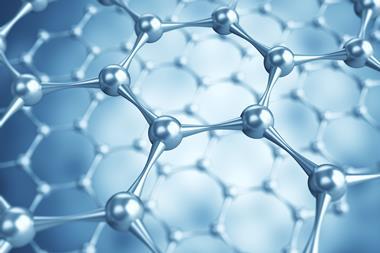
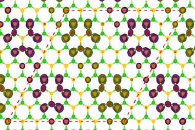
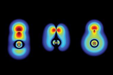
While 2D materials ‘are currently where we were about 10 years ago with graphene’ according to Novoselov, he’s enthusiastic about the prospects of stacking different types to build heterostructures. He emphasises that a variety of different electronic devices have emerged from academic research, including transistors and light-emitting diodes. Stacking individual 2D crystals means scientists can use the properties of those materials to do things traditional semiconductor heterostructures can’t.
‘When you stack 2D materials, it’s almost like designing materials atom by atom, on demand,’ observes Kirill Bolotin from Vanderbilt University in Nashville, US, who isn’t directly associated with the NGI. ‘It’s not exactly the first time humans have been able to do this, but it was ridiculously expensive. Stacking 2D materials is more-or-less easily accessible technology.’ Novoselov and his NGI colleagues are among those who ‘lead the way for the entire field’ he adds.
References
K S Novoselov et al, Science, 2016, DOI: 10.1126/science.aac9439


No comments yet