

With rock-solid stability and rapidly improving efficiency, could a mineral-derived photovoltaic material called kesterite finally push thin film solar into the mainstream? James Mitchell Crow talks to the experts
-
Kesterite’s solar potential: Kesterite, a mineral-derived photovoltaic material, is gaining attention for its low cost, earth-abundant, non-toxic composition and excellent stability – making it a promising alternative to existing thin-film solar technologies like CIGS and cadmium telluride.
-
Efficiency breakthroughs: After a decade-long plateau at 12.6% power conversion efficiency (PCE), recent innovations have pushed it to nearly 17%, with expectations to reach 20% within five years – crossing the threshold for commercial viability.
-
Chemical and crystallisation advances: Progress has come through chemical solution processing, solvent innovations (especially using 2‑methoxyethanol) and precise control of crystallisation and defect suppression during fabrication, including alloying and hydrogen treatments.
-
Tandem cell promise: Kesterite’s compatibility with silicon makes it a strong candidate for tandem solar cells, especially in wide-bandgap configurations, potentially enabling higher energy conversion at low cost and with minimal toxicity.
This summary was generated by AI and checked by a human editor
There’s a familiar ring to the origin story of kesterite, the latest would-be solar super-material.
Kesterite was discovered when geologists working a remote Russian mountain range came upon an unusual mineral with a distinct metallic lustre, and took a sample back to the lab for analysis. Decades later, researchers in Japan demonstrated that semiconducting thin films of kesterite had photovoltaic (PV) properties, and concluded that it had potential as a very low cost solar cell.
So far, so perovskite: another promising thin-film PV pioneered in Japan, derived from a mineral unearthed from a Russian mountainside. But from the point in each story where researchers first demonstrated a light-induced trickle of electricity from each material, the two tales could hardly be more different.
PV perovskite proved so amenable to researchers’ enhancements, its solar power conversion efficiency (PCE) rose with unprecedented speed, exceeding 20% within 10 years and continuing to climb. Kesterite’s solar efficiency, in contrast, climbed slowly to 12.6% then stalled completely, not budging for a decade.
In 2022, researchers finally broke through kesterite’s PCE ceiling to reach 13% – and the kesterite community’s luck finally changed. In the past three years, a string of record-breaking kesterites have pushed its PCE upward with perovskite-like speed. The latest materials almost touch 17%, and further gains are imminently expected, says Qingbo Meng, who directs the Center for Clean Energy at the Chinese Academy of Sciences in Beijing and whose team holds the current kesterite PCE record.
‘We entered the kesterite solar cell field when the efficiency was only around 5%,’ Meng says. ‘Today, certified efficiencies have exceeded 16%, with an average annual increase of nearly 1 percentage point.’ Within the next five years, he says, kesterite solar cell efficiency should reach or exceed 20%, crossing the threshold to commercial viability.
The right chemistry
During kesterite’s dark decade, many in the field conceded defeat with the recalcitrant material and went to work on perovskites instead. For the few researchers who never quit kesterite research, the material’s shining potential upsides as a solar technology stopped them from stepping away.
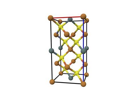
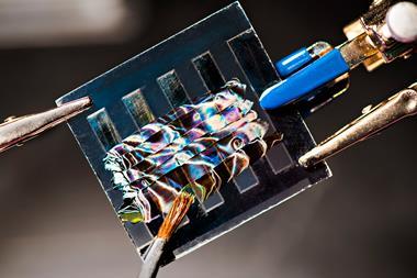
Kesterite PV combines copper, zinc and tin with the chalcogen ions sulfur, selenium or a blend of both, in the formula Cu2 ZnSn(S,Se)4 – gaining it the nickname CZTSSe. Each element in kesterite is inexpensive, earth-abundant and non-toxic – characteristics it shares with silicon but few other solar materials.
These attributes give kesterite an advantage over two already-commercialised thin film solar technologies, says kesterite researcher Alice Sheppard, who recently completed her PhD with David Fermin at the University of Bristol, UK. Copper-indium-gallium-selenide (CIGS) solar cells contains two scare elements, indium and gallium. ‘As for cadmium telluride solar, tellurium is scarce and cadmium is toxic,’ she says. Both technologies have remained relatively niche products in the global PV market.
Kesterite’s makeup also gives it theoretical advantages over photovoltaic perovskites, and not just because the best ones contain toxic lead. The fourth key property that kesterite solar shares with silicon is excellent stability. Kesterite PV is a thin film of virtually the same stuff dug from the Russian mountainside, just with zinc in place of the original mineral’s iron. ‘Kesterite is inherently stable at room temperature,’ Fermin says.
Photovoltaic perovskite, in contrast, is a hybrid combination of organic and inorganic ions such as methylammonium, lead and iodide, which shares only its crystal structure with the parent mineral. The ions in these hybrid materials are prone to drift out of position in the crystal lattice, leaving performance-sapping defects.
‘The thermodynamically stable phase of perovskite is one in which lead iodide goes one way and the methyl ammonium goes the other way,’ Fermin says. This structural instability can be accelerated by heat, light and moisture, which can rapidly degrade perovskite solar performance. In accelerated degradation tests, perovskite PCE can decline rapidly. ‘Kesterites start lower, but keep on going,’ Fermin says.
Defeating defects
If kesterite’s starting efficiency could be pushed to a higher number, its broad attributes suggest a bright future. The key factor still limiting kesterite PCE – which despite recent gains, remains far below its 32% theoretical maximum – is not defects that develop during its operation, but those formed during its fabrication. ‘The issue since the beginning has been how to ensure that each element goes into the right place in the crystal lattice,’ says Fermin.
Among thin film semiconductors, kesterite fabrication poses a particular challenge, says David Mitzi, a photovoltaic materials researcher at Duke University in North Carolina, US. ‘With kesterite, the metal ions all have roughly the same ionic size, and they have the same preferred coordination, so they readily switch sites in the crystal lattice,’ Mitzi says. ‘This creates disorder that can introduce electronic defects that in turn can reduce photovoltaic performance.’
Adding to the challenge, there is a characterisation technology gap for studying structural defects and their effects in a material as complex as kesterite. ‘Even for simpler materials, it’s not easy – but when you’ve got four, five or more elements, understanding what is driving performance degradation is very difficult,’ Mitzi says.
The dearth of characterisation methods for kesterite defect analysis is the crux of kesterite solar’s slow development, Fermin says. ‘We know, for instance, that copper and zinc can swap places, and that tin can go into the wrong place - but we don’t know how much these things happen or how bad they are,’ he says.
What techniques we do have to detect defects in kesterite can’t quantify them, so can’t guide efforts to improve performance. ‘There can be absolutely no difference in the Raman spectrum, electron microscopy and X-ray diffraction analysis of a kesterite that gives you 2% efficiency and one that gives you 15%,’ Fermin says.
Computational analysis has also been of limited use, Meng adds. ‘Although theoretical models predict several defect types, there is significant inconsistency with experimental results, primarily due to discrepancies between theoretical crystallization models and actual CZTSSe growth processes,’ he says. ‘We therefore focus on experimentally establishing direct correlations between defect types and device performance.’ Gains in kesterite performance have come at the expensive of extensive experimental effort, and a lot of trial and error.
Before joining Duke, Mitzi worked at IBM, where he led the team that pushed kesterite performance above 9.6% in 2010, and then to 12.6% in 2013 – setting the performance benchmark that would last for a decade. Among the team’s innovations, the key step was developing a benchmark solution processing method for growing the kesterite thin film. ‘That process, based on hydrazine as a solvent, provided a facile pathway to clean films with very nice grain structure that were very amenable to getting to high performance,’ Mitzi says.
The team also optimised the material’s ratio of sulfur to selenium to tune its bandgap for maximum energy capture from sunlight, and borrowed methods from CIGS manufacture to passivate surface defects. ‘Beyond these things, it was just a lot of work, making thousands of devices to get to the point where you can reproducibly make them with high performance,’ Mitzi says. Shortly after completing the project, Mitzi stepped away from kesterite research after leaving IBM for academia (see box Size matters below).
Size matters
Shortly after setting the 2013 kesterite solar performance record that would stand for almost a decade, thin film PV researcher David Mitzi left his position at IBM to join Duke University. At the same time, Mitzi refocused his research on alternate thin film PV materials – and not just for a clean break from his former industry role, he says. ‘What I like to work on is discovering new materials,’ he says.
The recent history of PV research and development highlights the importance of continuing to explore new materials, Mitzi says. ‘Success in a solar technology depends on a lot more than just demonstrating a high performing device,’ he says – noting PV perovskite’s ongoing instability issues.
One direction we’ve worked in is replacing the zinc with barium
To successfully commercialise a PV product, manufacturing factors including reproducibility, yield, cost, materials availability and the compatibility of a new fabrication process with existing manufacturing facilities are all important, Mitzi says. ‘An example of that is CIGS, which can get to high performance, but hasn’t been able to compete with cadmium telluride and other solar technologies because it is a more complex material, harder to manufacture reproducibly using a high throughput process.’
To expand the available options, Mitzi has explored materials close to kesterite but that should be less inherently prone to defects during their fabrication. ‘In kesterite, the similar ionic size and chemical behaviour of copper, zinc and tin facilitate their swapping of sites, creating defects,’ Mitzi says. ‘One direction we’ve worked in is replacing the zinc with barium, a much larger atom that generally has different preferred coordination than zinc.’
As kesterite’s most important electronic conduction bands derive mainly from the copper, tin and the chalcogens in the material, switching out the zinc should reduce certain defects while maintaining a similar electronic band structure enabling PV performance, Mitzi rationalised. So far, his team has got these materials up to around 6% solar efficiency. ‘That needs to go higher – but I think the work furthers the understanding of how crystal structure can be used to control defects toward higher performing materials,’ he says.
Finding chemical solutions
Among thin film PV materials, making high quality kesterite PV is particularly reliant on getting the chemistry right.
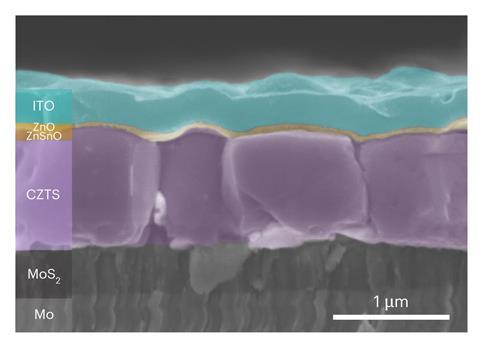
As a broad family, these materials can be made by physical means, via vacuum deposition of precursors onto a substrate. Alternatively, they can be made chemically, coating the substrate with a solvent-based ‘ink’ of the precursors, then allowing the PV film to crystalise as the ink dries during a heat-based annealing step.
‘In all other thin film PV technologies, the best performing devices are made by vacuum-based physical vapor deposition,’ Fermin says. But for kesterite PV, the record-breaking materials have all been made by chemical solution processing.
It’s an observation that points to the key role that chemical complexes pre-formed in the ink can play in minimising structural defects as the kesterite crystalises, Fermin says. ‘We and others have shown that just by changing something like a zinc acetate to a zinc chloride in the precursor solution, you can change the performance of the device by several percentage points – it’s absolutely remarkable.’
The choice of solvent also seems to shape the precursor complexes that form in the ink, influencing the quality of the resulting kesterite film and its PV performance, Fermin and Sheppard have found. In one study, they showed they could control the distribution of tin in a kesterite film – and boost device PCE almost two percentage points – by adjusting the ratio of a cosolvent mixture of isopropanol and dimethylformamide.
The lack of resources severely hindered technical progress in this area – but work in the field never ceased
Kesterite’s strong solvent dependency posed a major problem for researchers looking to push kesterite PV performance past Mitzi’s 12.6% record, set using hydrazine. As a carbon-free solvent, hydrazine was in many ways ideal for making clean, high quality, residue-free kesterite films. But it is also explosive and highly toxic. ‘Hydrazine-based solvents are extremely hazardous, making it difficult for many teams to conduct similar research due to safety concerns,’ Meng says.
Having to rework kesterite production to use more environmentally friendly – but less fabrication-friendly – solvents proved to be a major setback in kesterite PV performance. Confounding the field, innovative approaches to supress defects and boost kesterite PCE failed to show the anticipated benefits.
The longer that kesterite PV remained in the doldrums, the more researchers and funders jumped ship – often into perovskite research. ‘The lack of human and financial resources severely hindered technical progress in this area,’ Meng says. ‘Nevertheless, exploratory work in the field never ceased.’
Searching for an alternative solvent to hydrazine, Meng and his collaborators focused on dimethyl sulfoxide (DMSO) and 2‑methoxyethanol (MOE). ‘Developing a new baseline process with these less-easy solvents, that allow testing one parameter at a time to start progressing step by step to higher performance, was crucial to our record finally being broken,’ says Mitzi.
Kesterite PCEs began slowly climbing again, and in 2022 Meng and his collaborators reported a device with 13% PCE. ‘After eight years of relentless effort, solar cells fabricated with DMSO-based eco-friendly solutions broke the 12.6% efficiency record,’ Meng says.
Increasingly, the field has settled on MOE as the best solvent, and all kesterite PCE records subsequently set have all used MOE. There seems to be something special about MOE, Sheppard says. ‘We think there’s complexation in there which just doesn’t happens in other solvents,’ she says. Understanding MOE’s magic is a current focus of Sheppard and Fermin’s research.
Crystallisation maze
Beyond the precursor ink, controlling the chemistry as the kesterite crystallises during thermal annealing is essential for growing high quality thin films, Meng says. ‘Since these materials crystallise via solid-state reactions, we believe precise control of the crystallisation process is essential for effective defect suppression,’ he says.
Kesterite PV annealing typically involves heating the film in selenium or sulfur vapour, to incorporate the correct ratio of chalcogenide into the final material. Mastering selenisation to minimise selenium vacancies in the material is one focus of Meng’s work. Selenium vacancies are one of the main factors limiting kesterite efficiency, he says.
‘Selenium vacancies mainly originate from selenium loss during the later stages of selenisation,’ Meng says. ‘We have introduced surface compound coatings to effectively inhibit selenium evaporation and reduce defect levels.’ Fully controlling the selenisation step remains the team’s core research direction, he adds.
The team suspected that incomplete cation exchange during crystallisation, leaving metal ions in the wrong spot in the final material, was another likely source of defects. They showed that multicomponent elemental alloying – adding small amounts of other metals into the precursor ink – could weaken metal–chalcogenide bonds and accelerate atomic exchange. The strategy boosted kesterite PCE to a new record of 14.6%, the team reported.
Most recently, the team used alloying to deliberately introduce benign vacancies in the kesterite surface, freeing up copper and zinc ions to swap into the correct position during annealing. The technique improved copper–zinc order by enabling the two ions to swap positions in stepwise fashion via a vacant site rather than in a single concerted step, and pushed device PCE to 15.4%, the team says.
Mastering the tandem
For Xiaojing Hao, a kesterite PV researcher at the University of New South Wales, Australia, the potentially perfect pairing that kesterite could make with silicon is what drives her work.
‘Ever since starting my PhD, I have been working to find a top cell that you can partner with silicon for next generation tandem cells,’ Hao says. ‘Silicon is earth-abundant, non-toxic and stable, and so is kesterite, so it’s potentially a really good material.’
Combining silicon with a ‘wide bandgap’ kesterite, which efficiently captures higher energy wavelengths of sunlight toward the ultraviolet end of the spectrum, should result in a tandem cell that converts more solar energy into electricity for minimal additional cost. Kesterite that uses only sulfur rather than a sulfur–selenium blend is naturally a wide bandgap material.
Hao’s latest innovation shows that, in addition to fine-tuning the kesterite precursor ink and engineering the crystallisation, a third step during kesterite manufacture can improve film quality and boost kesterite PV performance.
The method was inspired by conventional silicon solar cell manufacture, where hydrogen treatment is used to passivate defects in the silicon and improve its stability. Hydrogen treatment can also push oxygen out of the material.
In kesterite, oxygen isn’t a big problem. But the sodium ions that the oxygen is usually found stuck to can be. ‘Kesterite can contain a lot of sodium, which diffuses into the material from the sodalime glass used as a kesterite solar cell substrate,’ Hao says. ‘If you have a lot of sodium, that can cause a problem.’
Sodium’s association with oxygen offered a chance to sweep it aside, Hao realised. ‘We know that oxygen can be driven out by hydrogen – so we thought, let’s see whether the hydrogen can move this sodium via the oxygen,’ Hao says. ‘And we found it works.’ Hydrogen treatment drove the sodium from the crystal bulk to the surface – where its presence can benefit the material’s surface conductivity and enhance the efficiency of the resulting kesterite solar cell.
Hao demonstrated the effect in wide-bandgap kesterite – where PCE had been stuck at 11% since 2018. The team initially pushed wide bandgap kesterite PCE to 11.4%, but has already gone higher. ‘Hydrogen annealing is like a baseline for us now because we know it works very well,’ she says. The team’s latest certified materials have jumped to 13.2%.
The hydrogen treatment step also works on CIGS solar cells, the team has shown – so it should certainly be applicable to other types of kesterite, used in combination with recent ink formulation and crystal engineering advances, Hao says. ‘Low bandgap kesterite also has the sodium problem, so I think the hydrogen should work for them as well,’ she says.
Recent progress has reenergised the field to keep pushing kesterite research forward, Hao says. ‘Everyone is really excited about it, and the discussion is very active.’
‘This rapid progress gives me great confidence for the future,’ Meng says. ‘As the advantages of kesterite technology become more widely recognized, I believe funding and talent will return to the field, driving further breakthroughs.’
The energy now flowing back into kesterite research is a marked turnaround from the situation five years ago, when nothing seemed to be working, Hao says. With reliable new baseline methods for high quality kesterite fabrication now in hand, many of these ideas would be worth revisiting.
‘It’s like a bucket with lots of holes in – patching the smaller holes barely has any effect when you have a lot of water leaking out through the big ones,’ Hao says. With several big holes in kesterite performance now fixed, patching the smaller ones should now have a much more noticeable impact.
Given kesterite’s fundamental strengths as a low cost, non-toxic, earth abundant, stable material, if its efficiency can be pushed just a little higher, its PV future could be very bright, Hao says. ‘If we can get it to 20% efficiency then I think it will really take off, since it meets all the criteria for the type of material we want to be using.’
Despite its humble mineral origins, perhaps kesterite will be the thin film solar story with the trope-defying happy ending.
James Mitchell Crow is a science writer based in Melbourne, Australia


No comments yet