
Defects may actually help improve working of popular photovoltaic device
Scientists in the US have imaged the tortuous journey current takes through a cadmium telluride solar cell as it is exposed to light. Such a map may help shed light on how defects can affect a CdTe cell.
CdTe devices are the second most popular photovoltaic technology in the world, holding 5% of the global market. It’s a sizeable market share, but one dwarfed by silicon-based cells, which occupy 85%.
Touted as a cheap alternative to silicon, CdTe are set to take more of this market as their efficiencies rise. But it’s been a very slow rise up to this point. ‘They are not nearly as efficient as they can be and explanations as to why have varied over the past couple of decades,’ says Bryan Huey from the University of Connecticut.
One explanation for this stems from CdTe’s microstructure – an issue that is often ignored on a production scale. ‘Many measurements are made, from the industrial perspective, on the metre square, house-sized, panel- sized scale,’ explains Huey. ‘If we’re talking about scaling up solar cells … then if we’ve got lots of regions that are underperforming by an order of magnitude, that’s a very clear path forward for improving performance.’
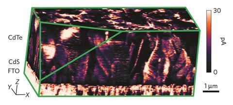
Huey’s team has now delved into a functioning CdTe cell using a modified form of atomic force microscopy (AFM). With AFM, researchers can obtain atomic resolution images of surfaces by passing a probe tip across it and recording its deflection, like a turntable needle passing over a vinyl record.
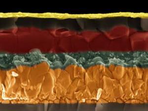
To measure the current passing through the solar cell, which is a CdTe light harvesting layer sandwiched between two electrodes, the team removed one of the electrodes. ‘The AFM tip acts as a positional electrode,’ says Huey. When light is shone on the cell, the AFM tip completes a circuit and the current flowing between the back electrode and tip is measured. ‘It’s an almost complete solar cell.’
But the diamond-coated tip also doubles up as a microscale chisel. As the tip is moved across the surface, it removes material layer-by layer, allowing the team to dig deeper into the CdTe structure. Once finished, the team has a 3D image of current flow between grains that resembles a time lapse of a night-time cityscape.
The images suggest that planar defects, such as grain boundaries and irregular lattice stacking, may actually support current flow in the cells. ‘It wasn’t understood how important various defects are to the local properties until now,’ Huey comments. ‘We definitely nailed that planar defects, in particular, are extremely active.’
Although the technique is very effective, the role of grain boundaries and defects in CdTe cells is a divisive issue, according to Jon Major, a photovoltaics expert from University of Liverpool, UK. ‘This is by no means the definite answer though as various techniques have shown either positive or negative aspects of CdTe grain boundaries,’ Major tells Chemistry World. ‘It will take a lot more work using various contrasting techniques before we can truly understand grain boundary functionality.’
References
J Luria et al, Nat. Energy, 2016, DOI: 10.1038/nenergy.2016.150


No comments yet